| WR Home Topic Home | Chapter: 1 |
| <Previous | Next> |
Chapter 01
Page 9
A short note on Atmega328P registers
In computer architecture, a processor register is a small amount of storage available as part of a CPU/ALU/processor/IC. Registers are temporary memory locations built inside the micro-controllers. Registers can be accessed more quickly as compared to other memory.
In the microcontroller Atmega328P, there are three ports B, C & D.
Each of the port is "associated" with THREE registers
(so there are NINE registers)
- Data Direction Registers (Configures the pins as Output or Input pins): DDRB, DDRC, DDRD
- Output Registers: PORTB, PORTC, PORTD
- Input Registers: PINB, PINC, PIND
Lets start with an example:
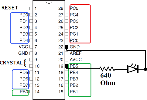
Suppose, a developer needs to connect an LED to the microcontroller. If the LED is connected to the microcontroller "properly", then it can be switched ON/OFF via a program OR can be blinked ON-OFF-ON-OFF .........., even its blink-rate can be programmatically controlled. In order to do so, the developer needs to connect the LED to a General Purpose Input Output pin as shown below:

Here the LED is connected on the 6th pin of PORTB. The name of the six’th pin is PB5, as the pin numbers start from zero, rembember PB0 to PB7 were the 8-pins.
LED is a output device. The data/signal will flow from micro-controllor to outside. So, the developer needs to specify that PB5 is an output pin. At a particular time instant a pin can either act as an input pin OR an output pin, but not both. The data direction can be specified with the help of a control register, which has nothing to do with the data itself, but the direction of data. Hence it is call a Data Direction Register or DDR in short. Since there are three ports B,C & D, there are three data direction registers: DDRB, DDRC & DDRD
- DDRB
This governs which of the 8-pins of Port B, will act as input and which will act as output. DDRB stands for Data Direction Register for B. This is a control register, the developer can programmatically write in it to define the direction of data, whether Input or Output. The 8-bits of this register defines the direction of 8-pins in the port. If any bit of this register is SET (i.e. made 1) then the corresponding PIN on the PORT becomes an output PIN (Now it is a different matter that a ZERO is outputted or a ONE is outputted to the port; this registers just defines the "direction" of data, it has nothing to do with "what is the data" to be outputted). Similarly if any BIT of this register is CLEARed then that pin acts as input pin.
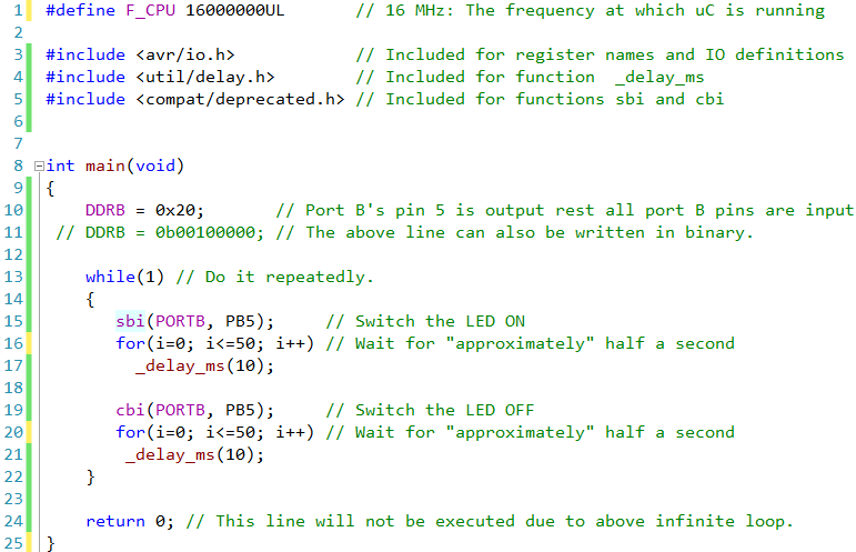
As per the above example if DDRB = 0x20, it means that only pin 5 is output pin, rest are input pins.
More Examples:
DDRB = 0x00 means that all pins of PORT-B are input pins
DDRB = 0xFF means that all pins of PORT-B are output pins
If four LEDs are to be connected on lower nibble of the PORT B (PB3, PB2, PB1, PB0) then and four switches are to be connected to upper nibble of PORT B then:
DDRB= 0x0F as switches are input devices. A zero in the DDR indicates the data direction as input.
- PORTB (8-bit register)
If any data is written to this register, the data reaches the Port-B. So whenever some data is to be send, OUT to Port-B of microcontroller then this register is used.
- PINB (8-bit register)
If any data is to be READ from PORT-B then this register is used. In other words if any data is to be INPUTTED from PORT-B then this register is used. For the current LED example this register will not be used. but if a switch was to used as an input device, we could have read the status of the switch (Pushed or not, ON or OFF etc) from this register.
Now consider the following program. It switches on the LED for 0.5 second and switches it off for 0.5 second.

NOTE: This example used the pin PB5 (Arduino: Digital Pin 13) because the Arduino board already has a LED connected to this pin.
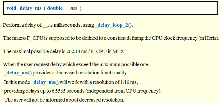
To use a delay for 500ms (or 0.5 sec) : A 10ms delay was called 50 times.
WHY ?
Bacause:

NOTE: The software WinAVR has an excellent documentation on library files (header files) Once WinAVR is installed the typical path to find the help files is: C:\WinAVR-20100110\doc\avr-libc\avr-libc-user-manual\index.html (Click on Library Reference, then click on <util/delay.h> An online version of the is here.
| WR Home Topic Home | Chapter: 1 |
| <Previous | Next> |