| WR Home Topic Home | Chapter: 1 2 3 4 5 6 |
| <Previous | Next> |
Chapter 06
Circuitry for Base PCB
Page 1

Purpose of base PCB
This circuit performs two tasks:
- First is to generate AC power and to feed it to centre taped transformer.
- Second is to drive a DC motor with variable speed.
Component Description
Main components:
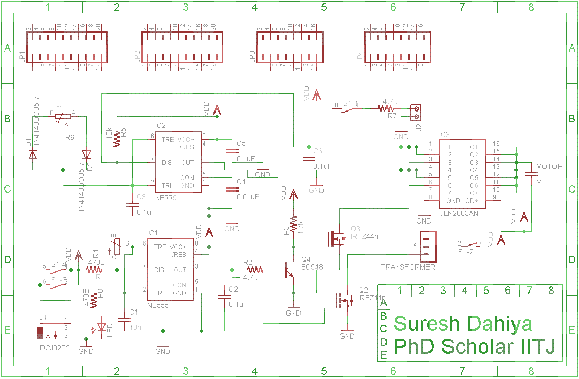
- NE555: This most common timer IC. In this circuit, two NE555 ICs are used. In this circuit both ICs are used to generate square wave output in astable mode.
- BC548: This is general purpose switching transistor and it is used to generated a inverted output signal from a square wave input.
- IRFZ44N: This is low cost power MOSFET. In this circuit, two MOSFETs are used and each of them drives half part of the primary coil.
- ULN2003: This is a general purpose driver IC. It is used here to drive base motor.
Circuit Working: Part I
- IC1 NE555 timer is used as astable oscillator which generates square wave as per standard astable oscillator configuration given in its datasheet.
- A power indication LED, DC jack for power supply and power ON-OFF button is provided in the circuit.
- Square wave output from IC1 is fed to transistor BC548 to give inverted output at it’s collector terminal.
- Both inverted and non-inverted square waves are fed into separate MOSFETs IRFZ44n. Each of MOSFETs drives current in half part of the primary coil of transformer.
- Centre point of primary coil is connected to positive terminal of power supply. End points of the primary coil are connected to ground one by one through MOSFETs due to switching action of MOSFETs. Thus overall DC current in primary coil is zero and there is only AC current in from of square wave.
Circuit Working: Part II
- IC2 NE555 timer is used in astable mode but with slight modification in standard configuration to have full control on duty cycle of output square wave.
- In this case final output is available at pin7 while output of pin3 is used for feedback to control duty cycle.
- Two diodes D1 and D2, having low threshold voltage, are used in feedback path to give feedback to trigger pin of IC2.
- Final output of atable oscillator drives ULN2003 to control speed of the base motor.
PCB: component placement considerations
- MOSFETs are placed in one side of PCB near the boundary so that they can easily dissipate heat and may not damage other sensitive components.
- Few extra connectors are placed for general purpose modifications in the circuit.
- High power terminal for primary coil are placed at optimum distance from the MOSFETs.
PCB: Track width and routing considerations
- Angles in tracks should not be not sharper than 45 degree.
- Power tracks should be always thicker. Thickness depends upon current rating and available routing space.
- Power tracks should note make a closed loop around circuit means both positive and negative tracks should run in same direction either in clock-wise or anti clock-wise.
- Signal tracks can be thin below 0.25mm. However if sufficient space is available and purpose is not commercial then signal tracks can also have width up to 1mm.
- Manual routing is most important part in track routing so after primary auto routing manual routing is suggested to cover above considerations
| WR Home Topic Home | Chapter: 1 2 3 4 5 6 |
| <Previous | Next> |